Parasitic Extraction Tools
| Schematic | SPICE | Physical Design | Verification | Parasitic Extraction | Signal Integrity |
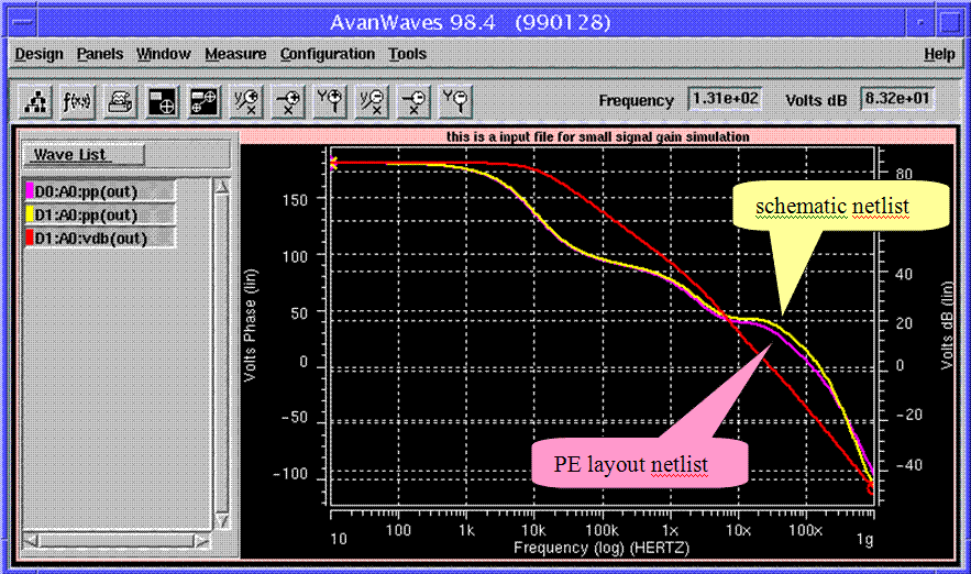
In deep sub-micron technology, interconnect parasitic effects of layout are having more and more influence on the performance of circuit designs. Zeni PE provides layout engineers the capability to perform highly accurate parasitic capacitance, resistance and inductance extraction on full-chip layouts, selected area, or a single net.
Zeni PE's Features and Benefits
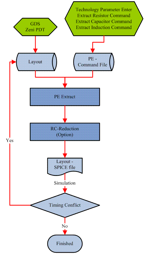
Zeni PE is built on a foundation of proprietary algorithms with BEM (Boundary Element Method) and Curve-Fit Method to achieve high computation speed and accuracy. The quasi-3D capacitance extraction guarantees an error range less than 10% while maintaining the runtime in a fast linear-complexity speed. Its seamless integration with Zeni Veri makes it possible to directly generate a netlist file containing parasitic parameters from GDSII layout data. Only the process parameters and extraction commands are necessary in command files; there is no need to include sophisticated equations or formulas. The parasitic extraction results are marked at the corresponding places on the layout to facilitate the searching of nodes and devices. It also support interactive extraction of RC parasitic elements for nets selected in Zeni PDT, and the result will be passed to Zeni SI for interconnect timing analysis, noise analysis and RC reduction.
Relationship Between Extraction Results and Layout
In Zeni PDT, commands such as Show-Device & Node and Which-Device & Node can locate and display nodes for parasitic device terminals and their corresponding layout location. This is useful for the parasitic resistor extraction since parasitic resistor extraction will change the nodes in the original layout. The relationship between the original circuit nodes and the extracted circuit nodes can be easily traced along with devices and nodes both in original layout and schematic views.
Parasitic Resistor Extraction
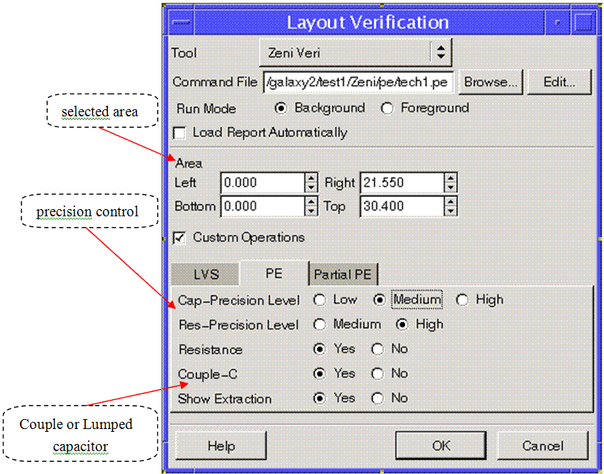
Since parasitic resistor elements only depend on the shape of the layout geometries and the layer conductance, it is easier to calculate the parasitic resistor elements than it is to calculate the parasitic capacitor and parasitic inductor elements. Zeni PE can calculate the parasitic resistor elements with two levels of precision, with the higher precision setting taking longer runtime.
Parasitic Capacitor Extraction
Quasi-3D parasitic extraction sweeps any 3-D structure in multiple passes and includes geometry superposition. It treats overlap capacitors, lateral capacitors and fringe capacitors differently. Thus it is much more accurate than 2-D parasitic extraction. The methodology used for calculating parasitic capacitance is very important. Numerical modeling utilizes field solver to extract the parasitic capacitance in order to achieve the maximum accuracy. While it can handle very complex 3-D structures, sometimes it can be too slow for full chip parasitic extraction. Recently, a lot of research has been done on numerical modeling because of the development of deep sub-micron technologies. The main reason for this is that the connectivity delay has become the dominating delay as the feature size keeps reducing. In addition, new process techniques such as Air Gap, Conformal Oxide and Shallow Trench Isolation, Stacked Structures and Fin Structures will lead to very complicated analytical models. It makes a 3-D field solver more valuable. Zeni PE uses a Quasi-3D extraction + Interpolation resulting in an excellent trade-off between high speed and high accuracy. Zeni PE can extract the parasitic capacitance with three levels of precision based on user requirements.
Parasitic Inductor Extraction
For high frequency integrated circuits, the parasitic inductance depends on the net's own layout geometry as well as the neighboring layout geometries. The calculated value also depends on the direction of the circuit path. Zeni PE can extract parasitic inductance and mutual inductance, and output it in SPICE format for post layout simulation and verification.


Email us with any other questions you may have: info(at)zeni-eda.com

