

Schematic Editor | Schematic Capture | Schematic Generator
| Schematic | SPICE | Physical Design | Verification | Parasitic Extraction | Signal Integrity |
Schematic Capture
Zeni Schematic Editor (ZeniSE) is a powerful schematic editor / schematic capture tool that supports hierarchical design, multi-window and multi-page editing. It supports import/export of industry standard netlist formats, as well as schematic data in EDIF format, thus allowing seamless interchange of schematics between other EDA tools. With many other useful features, ZeniSE offers a complete circuit design environment to finish sophisticated designs quickly and easily.

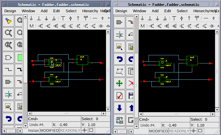
Multi-Window Editing
ZeniSE provides a multi-window co-editing feature. Designers can open more than one schematic window for same or different cellviews. This feature enables you to move or copy objects from one schematic cellview to others (see demo), or edit part of a cellview (zoom in) in one window while keeping an eye on the entire design in another window (see demo).
Multi-Page Editing
To facilitate designing large circuits, ZeniSE provides multi-page schematic editing features. Designers can partition a large schematic cellview into a number of “pages” connected by offpage pins, and each “page” contains a small but clear part of the whole design. Multi-page editing enables users to easily read and clearly print out large-scale designs page by page.

Bird's Eye View
Birds-eye view is a mini window showing the current schematic cellview’s panorama. Selecting an area in birds-eye view will show the corresponding part of the cellview in the schematic editor window, and vice versa. It improves the design efficiency significantly and is highly praised by our customers (see demo).
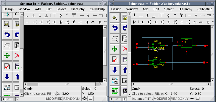
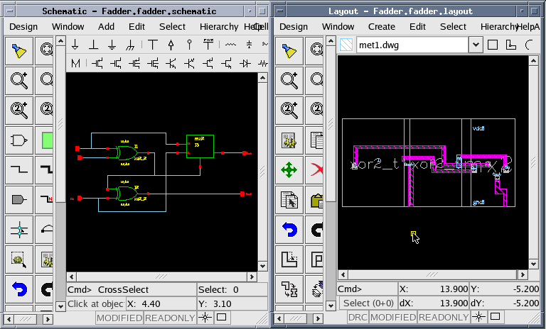
Cross Select
Cross Select is the key feature for the communication between the Zeni schematic editor and physical design tool. If designers select pins or instances in the schematic window or physical design window, the corresponding objects will be shown automatically in the other window (see demo).
Trace Net
Tracing nets in hierarchical schematic designs is a complicated, arduous and painful task, and sometimes it is almost unrealistic. The Trace Net feature will help designers locate and highlight net connectivity hierarchically and automatically with up to 6 different colors.

Import/Export EDIF Schematic
EDIF is an industry standard schematic interchange format that uses text to describe the design data. ZeniSE is able to translate EDIF files to schematic data, and vice versa. With this feature, our customers can seamlessly exchange their design data between Zeni and other EDA tools.

Import/Export Netlist - Schematic Generator
Beside EDIF, ZeniSE can also export schematic data in various standard and custom netlist formats, and import netlist in CDL, Verilog or mixed format to generate the corresponding schematic cellview. ZeniSE can therefore be used as a very effective schematic generator, and can create the complete schematic hierarchy from Verilog or CDL netlists.

Analog Simulation Deck
Simulation is a necessary process to verify the performance of the schematic design before moving to physical design. Analog Simulation Deck helps designers to easily setup various parameters required by the simulators. Furthermore, after finishing the simulation, designers can also probe critical signal nets on the schematic window with this environment.

Predefined Parasitic Loads
The standard design flow starts with an experienced circuit designer generating a schematic design. The designer must create his/her circuit with anticipated parasitic loads. This may be difficult since there is no way to drop in parasitic loads into the schematic. The designer must add resistor/capacitor loads for every net or take a significant risk by ignoring the loads during simulation. Then the parasitic loads must be removed to pass the schematic design to the layout engineer. At this point the layout engineer must complete the layout and perform Parasitic Extraction. The parasitics are back-annotated to the schematic and re-simulated by the circuit designer. The whole process cycles again as the designer tweaks the design and possibly makes layout suggestions.
The Pre-Defined Parasitic function in the system allows the circuit designer to simulate with pre-defined parasitics, pass the same schematic with design criteria to a layout engineer, and help the layout engineer to insure specification while the layout proceeds. The previous iterative process between schematic, layout, and back-annotation can be reduced to a single one-way flow.

Parasitic Parameter Back Annotation
PE Back Annotation can place the layout parasitic parameters on the corresponding schematic cellview. The easy to use interface, doesn't require any complex commands and operations, and provides a simple yet effective way to double check your design with real parasitic loads, and verify performace requirements are still being met.


Email us with any other questions you may have: info(at)zeni-eda.com